BegasBattleNotes
From DaphneWiki
(Difference between revisions)
(→UART (17F / MC68B50P)) |
(→Sync Generation) |
||
| Line 29: | Line 29: | ||
|15 | |15 | ||
|SC | |SC | ||
| - | | | + | |Stands for Sub-Carrier. Matches the color burst frequency. Runs at 3.58 MHz. |
|} | |} | ||
Revision as of 17:52, 26 October 2021
Contents |
Sync signals
Sync Generation
Video sync signals are generated by what appears to be a custom Sony chip called the CX 773A (I couldn't find any info about this by googling for it). You can find it on the Bega's Battle schematic called "DSP Control Decode" and it is at position 16K on the VDO-1 (bottom) PCB (the one with the two BNC outputs).
This custom IC takes in a 14.3182 MHZ clock and five of its output are used.
| Pin | Description | Notes |
| 4 | Composite Sync | Active low. Typical NTSC composite sync. Nothing unusual observed. |
| 6 | SG BLK | Active low. May refer to "signal block" meaning when to prevent computer generated video from going to the monitor. For top field, starts at beginning of line 1 and ends when line 21 begins, and otherwise goes low when HSync goes low (and lasts a little bit longer than HSync pulses). |
| 8 | HSYNC 2 | Active low. Appears to run at a constant 15.73 kHz frequency with no variation. Each line is 63.56 uS long. Each pulse lasts for 6.72 uS. Usually starts a little before csync and ends a little after. Goes low at the same time as SG BLK. |
| 11 | VSYNC 2 | Active low. For top field, starts at the beginning of line 1 and ends at the end of line 9. No apparent delay relative to csync. Each pulse lasts for 0.5721 ms and the frequency is a constant 59.93 Hz, with a period of 16.69 ms. |
| 15 | SC | Stands for Sub-Carrier. Matches the color burst frequency. Runs at 3.58 MHz. |
Signals from VDO-1 (bottom) PCB that are sent to Chroma board
| CN2 Pin from VDO-1 (bottom) PCB | CN1 Pin on Chroma PCB | Description |
| B3 | 2 | 12V |
| A5 | 3 | 5V |
| B5 | 3 | 5V |
| A7 | 9 | Analog red |
| B7 | 4 | DSP Sel (I assume this means whether to display laserdisc video or computer generated video) |
| A8 | 8 | Analog green |
| B8 | 5 | SUB PC BLKING aka BL (related to SG BLK) |
| A9 | 7 | Analog blue |
| B9 | 6 | csync |
| A10 | 1 | Ground |
| B10 | 10 | Ground |
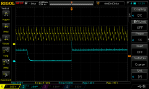
BNC output voltage levels
Yellow is SC (color burst?). Blue is csync. Blue averages about 2.4V high.
Serial I/O
VDO-2 CN2
| CN2 Pin from VDO-2 (top) PCB | Name | Notes |
| A1 | GND | |
| A2 | RxD | Incoming |
| A3 | TxD | Outgoing, +12V to -5V (apparently) |
| A4 | Tied to A5 | |
| A5 | Tied to A4 | |
| A6 | 12V | Through 1k resistor |
| A7 | GND | |
| A8 |
UART (17F / MC68B50P)
| Pin | Name | Notes |
| 1 | GND | |
| 2 | Rx Data | |
| 3 | Rx Clock | Tied to 16D-12 |
| 4 | Tx clock | Tied to 16D-12 |
| 5 | RTS' | Not connected |
| 6 | Tx Data | To 9J-2 |
| 7 | IRQ' | To main CPU IRQ (I think?) |
| 8 | CS0 | To 5V |
| 9 | CS2' | To 14E-9 |
| 10 | CS1 | To 5V? (schematic hard to read) |
| 11 | RS | Tied to an address bus line |
| 12 | VCC | To 5V |
| 13 | R/W' | To CPU R/W' it appears |
| 14 | E (Enable) | to something related to main CPU |
| 15-22 | D7-D0 | Data bus |
| 23 | DCD' | Tied to GND |
| 24 | CTS' | Tied to GND |
